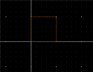
Find the overlapping shapes between three layers - Custom IC SKILL - Cadence Technology Forums - Cadence Community
Por um escritor misterioso
Last updated 02 setembro 2024
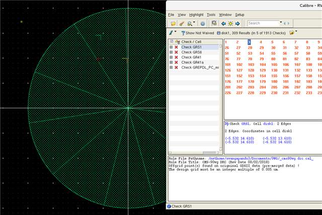
Creating Circles in layout - Custom IC Design - Cadence Technology Forums - Cadence Community

dbCreatePath unexpected additional line - Custom IC SKILL - Cadence Technology Forums - Cadence Community
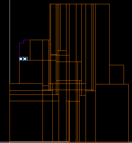
Merge BBOX in hierarchical layout - Custom IC SKILL - Cadence Technology Forums - Cadence Community
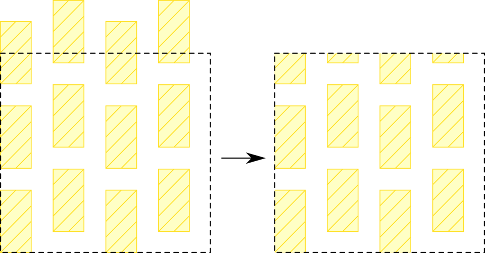
Clipping layer in Layout - Custom IC Design - Cadence Technology Forums - Cadence Community
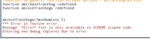
Different Behavior of leChopShape Command in ic 06.18.050 & in icadvm 18.10.090 !!! - Custom IC SKILL - Cadence Technology Forums - Cadence Community

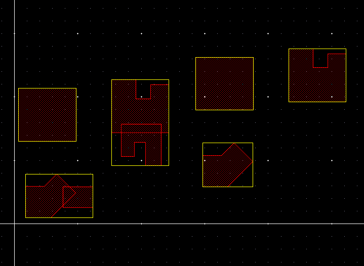
Find the area which not overlapped by some layer. - Custom IC SKILL - Cadence Technology Forums - Cadence Community

How to define a stop layer in connectivity for VIA - Custom IC SKILL - Cadence Technology Forums - Cadence Community
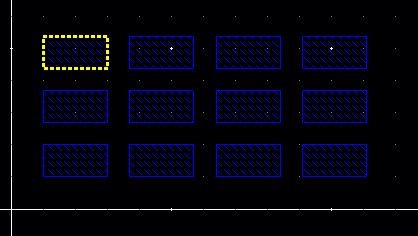
Skill code For designing layout for five different metal layers vias arranged in both X and Y axis. - Custom IC SKILL - Cadence Technology Forums - Cadence Community
Find the overlapping shapes between three layers - Custom IC SKILL - Cadence Technology Forums - Cadence Community
stop layout snapping two close by cells to overlap - Custom IC Design - Cadence Technology Forums - Cadence Community
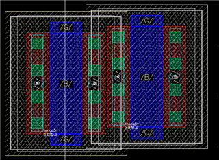
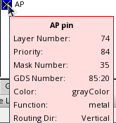
layout pin creation after binding the devices between schematic and layout - Custom IC SKILL - Cadence Technology Forums - Cadence Community
layout object purpose number directly? - Custom IC SKILL - Cadence Technology Forums - Cadence Community
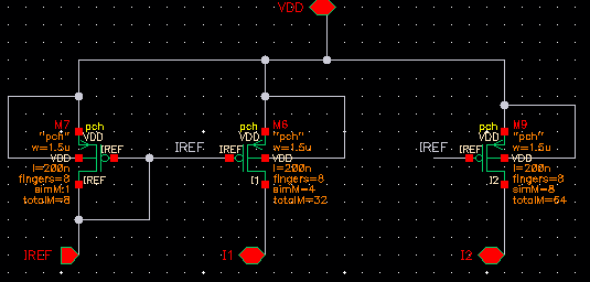
connect two metal nets - Custom IC SKILL - Cadence Technology Forums - Cadence Community
Recomendado para você
-
SMBOT no LinkedIn: 7 vantagens da SMBOT para seu negócio02 setembro 2024
-
 Apresentação da Plataforma de Tutoriais - SMBOT02 setembro 2024
 -
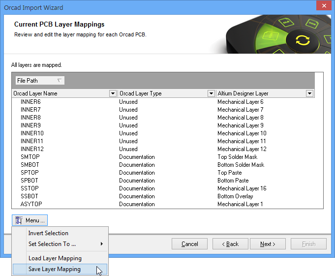 Importing a Design from OrCAD into Altium Designer02 setembro 2024
 -
SMBOT - Versão Mais Recente Para Android - Baixe Apk02 setembro 2024
-
SMBOT (@smchatbot)02 setembro 2024
-
Bem vindo(a) a SMBOT.mp4 on Vimeo02 setembro 2024
-
 HP EliteBook 8770W CPU Fan w/ Heatsinks 688733-001 653629-001 6043B011490102 setembro 2024
 -
 Chemical Guys CLY_403 - Clay Bar, Black (Heavy) (100 g)02 setembro 2024
 -
 Beware Productions - Coherent Distribution02 setembro 2024
 -
 raichu-uploads.s3.aws.com/logo_chatbot-maker02 setembro 2024


você pode gostar
-
 FAQ DO STEAM, Notícias02 setembro 2024
 -
 BONECA GRÁVIDA com bebe na barriga - Boneca barbie português - Joga comigo02 setembro 2024
 -
ip-loggers · GitHub Topics · GitHub02 setembro 2024
-
 Amy Meets Movie Sonic (sprites are not mine) : r/SonicTheHedgehog02 setembro 2024
 -
 Slendrina The Cellar (PC) Updated Full Gameplay02 setembro 2024
 -
 Black Clover: Sword of the Wizard King Releases Yuno Character Trailer02 setembro 2024
 -
Stream Meaning In Kannada - ಕನ್ನಡ ಅರ್ಥ02 setembro 2024
-
 Dishonored 2' Joins Other Bethesda Hits In The Xbox Game Pass Library02 setembro 2024
 -
 Sorry I'm Just Another Person Here — Luca + Text Posts 1/? - Luca Paguro02 setembro 2024
 -
 Assistir Fullmetal Alchemist Brotherhood Dublado Episodio 41 Online02 setembro 2024